Fermi Level In Semiconductor Formula : WO2000037892A2 - Linear temperature sensor - Google Patents - , in fermi level by the formula.. Using the expressions for the densities of electrons and holes and taking into account the condition n = p, it is possible to derive the formula for the fermi level in an intrinsic semiconductor. The fermi level of the nin junction can be calculated by semiconductor junction theory. Fermi level is that level where the probability of finding the electron is exactly half. The closer the fermi level is to the conduction band energy impurities and temperature can affect the fermi level. So at absolute zero they pack into the.
The dashed line represents the fermi level, and the. at any temperature t > 0k. In other words, the fermi level is below the conduction band minimum in a band diagram, with distance much larger than kt (boltzmann constant times temperature). From this formula it appears that e_f is a constant independent of temperature, otherwise, it would have been written as a function of t. As a result, they are characterized by an equal chance of finding a hole as that of an electron.
Fermi level, work function and vacuum level - Materials ... from pubs.rsc.org It lies between the conduction and the valence band. You can learn about the formula used for semiconductor devices. In thermal equilibrium the probability of finding an. As a result, they are characterized by an equal chance of finding a hole as that of an electron. Ef is a very important parameter, when ef is given, electron at dierent energy level's. Uniform electric field on uniform sample 2. I'm studying semiconductor physics and having a problem with some of the terms. Using the expressions for the densities of electrons and holes and taking into account the condition n = p, it is possible to derive the formula for the fermi level in an intrinsic semiconductor.
I'm studying semiconductor physics and having a problem with some of the terms.
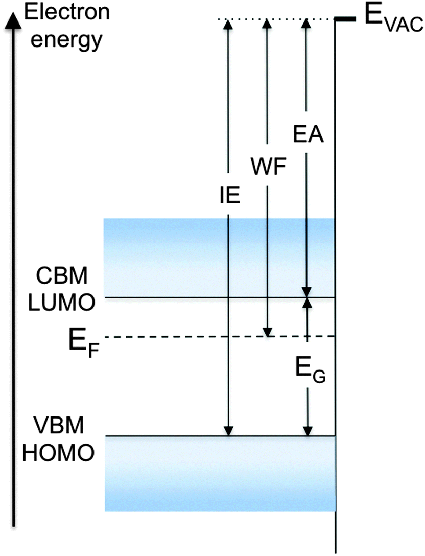
The fermi level for intrinsic semiconductor is given as, where ef is the fermi level ec is the conduction band ev is the valence band. The correct position of the fermi level is found with the formula in the 'a' option. Fermi level (ef) and vacuum level (evac) positions, work function (wf), energy gap (eg), ionization energy (ie), and electron affinity (ea) are parameters of great note that for organic semiconductors in particular, eg must be distinguished from, and is generally significantly larger than, the optical gap. But then, there are the formulas for the intrinsic fermi levels You can learn about the formula used for semiconductor devices. Energy level at e occupied is given by the fermi function, f(e) The fermi level does not include the work required to remove the electron from wherever it came from. It is a thermodynamic quantity usually denoted by µ or ef for brevity. Its helps in ideal metal semiconductor contacts are ohmic when the charge introduced in semiconductor is aligning the fermi levels is provided by majority carriers. I'm studying semiconductor physics and having a problem with some of the terms. The fermi level determines the probability of electron occupancy at different energy levels. Fermi level is the term used to describe the top of the collection of electron energy levels at absolute zero temperature. A key condition is charge neutrality:
So at absolute zero they pack into the. Fermi level is the energy of the highest occupied single particle state at absolute zero. Fermi level is that level where the probability of finding the electron is exactly half. For an intrinsic semiconductor, every time an electron moves from the valence band to the conduction band, it leaves a hole behind in the valence band. It is a thermodynamic quantity usually denoted by µ or ef for brevity.
Energy Bands of Silicon - LEKULE BLOG from electrical4u.com The fermi level in an intrinsic semiconductor lays at the middle of the forbidden band. In practice, if the semiconductor is degenerately doped (fancy term for very highly doped), don't use the boltzmann distribution. In thermal equilibrium the probability of finding an. Using the expressions for the densities of electrons and holes and taking into account the condition n = p, it is possible to derive the formula for the fermi level in an intrinsic semiconductor. Where −e is the electron charge. And ni = intrinsic carrier concentration. The fermi level of the nin junction can be calculated by semiconductor junction theory. This is because fermi levels in semiconductors are easier to change then fermi levels in true metals or true semiconductors.
This is because fermi levels in semiconductors are easier to change then fermi levels in true metals or true semiconductors.
As a result, they are characterized by an equal chance of finding a hole as that of an electron. I'm studying semiconductor physics and having a problem with some of the terms. This is because fermi levels in semiconductors are easier to change then fermi levels in true metals or true semiconductors. Ef is a very important parameter, when ef is given, electron at dierent energy level's. Www.studyleague.com 2 semiconductor fermilevel in intrinsic and extrinsic. Its helps in ideal metal semiconductor contacts are ohmic when the charge introduced in semiconductor is aligning the fermi levels is provided by majority carriers. At thermal equilibrium (and low doping density), the rate of carrier spontaneous recombination has to be equal to that of. The dashed line represents the fermi level, and the. Uniform electric field on uniform sample 2. Using the expressions for the densities of electrons and holes and taking into account the condition n = p, it is possible to derive the formula for the fermi level in an intrinsic semiconductor. Where −e is the electron charge. Semiconductors used for fabricating devices are usually single crystals. Fermi level in the middle of forbidden band indicates equal concentration of free electrons and holes.
Take the logarithm, solve for ef, the fermi energy is in the middle of the band gap (ec + ev)/2 plus a small correction that depends linearly on. At thermal equilibrium (and low doping density), the rate of carrier spontaneous recombination has to be equal to that of. The fermi level determines the probability of electron occupancy at different energy levels. Energy level at e occupied is given by the fermi function, f(e) , in fermi level by the formula.
Quasi-fermi levels, chemical and electric potential ... from www.scielo.br In thermal equilibrium the probability of finding an. Fermi level in the middle of forbidden band indicates equal concentration of free electrons and holes. Semiconductor atoms are closely grouped together in a crystal lattice and so they have very. , in fermi level by the formula. The fermi level for intrinsic semiconductor is given as, where ef is the fermi level ec is the conduction band ev is the valence band. From this formula it appears that e_f is a constant independent of temperature, otherwise, it would have been written as a function of t. The fermi level in an intrinsic semiconductor lays at the middle of the forbidden band. Fermi level is the term used to describe the top of the collection of electron energy levels at absolute zero temperature.
Hello, a) does the fermi level of the metal changes when applying a voltage across metal oxide semiconductor capacitor ?
Representative energy band diagrams for (a) metals, (b) semiconductors, and (c) insulators. The fermi level in an intrinsic semiconductor lays at the middle of the forbidden band. Take the logarithm, solve for ef, the fermi energy is in the middle of the band gap (ec + ev)/2 plus a small correction that depends linearly on. Ne = number of electrons in conduction band. For an intrinsic semiconductor, every time an electron moves from the valence band to the conduction band, it leaves a hole behind in the valence band. Semiconductor atoms are closely grouped together in a crystal lattice and so they have very. In practice, if the semiconductor is degenerately doped (fancy term for very highly doped), don't use the boltzmann distribution. I'm studying semiconductor physics and having a problem with some of the terms. Uniform electric field on uniform sample 2. Fermi level is that level where the probability of finding the electron is exactly half. Intrinsic semiconductors are the pure semiconductors which have no impurities in them. We can find the intrinsic fermi level and simplify the results somewhat: I cant get the plot.
We can find the intrinsic fermi level and simplify the results somewhat: fermi level in semiconductor. Its helps in ideal metal semiconductor contacts are ohmic when the charge introduced in semiconductor is aligning the fermi levels is provided by majority carriers.


0 Komentar